1Introduction
The PVX-4150 pulse generator produces fast, high voltage waveforms to 1,500 V. Optimized for high impedance capacitive loads, it is well suited for driving extraction grids and deflection plates for electrostatic modulation of particle beams in time-of-flight mass spectrometers and accelerators. Its robust and versatile design also makes it well suited for pulsing or gating power tube grids, Pockels cells and Q-switches, acoustic transducers, microchannel plates, photomultiplier tubes, and image intensifiers. The exceptional pulse fidelity of the PVX-4150 will optimize the performance of any system in which it is used.
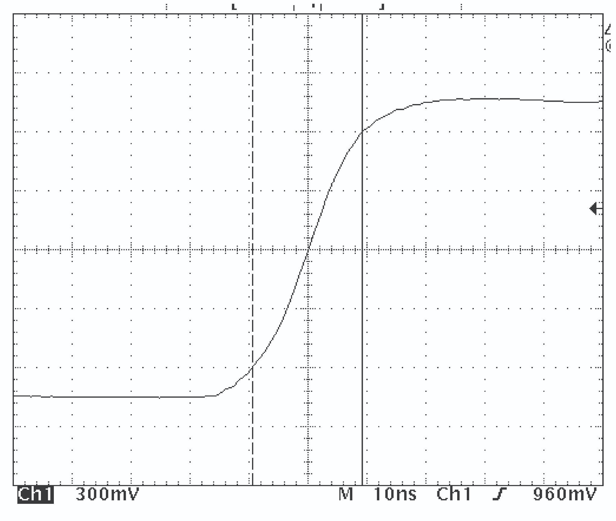
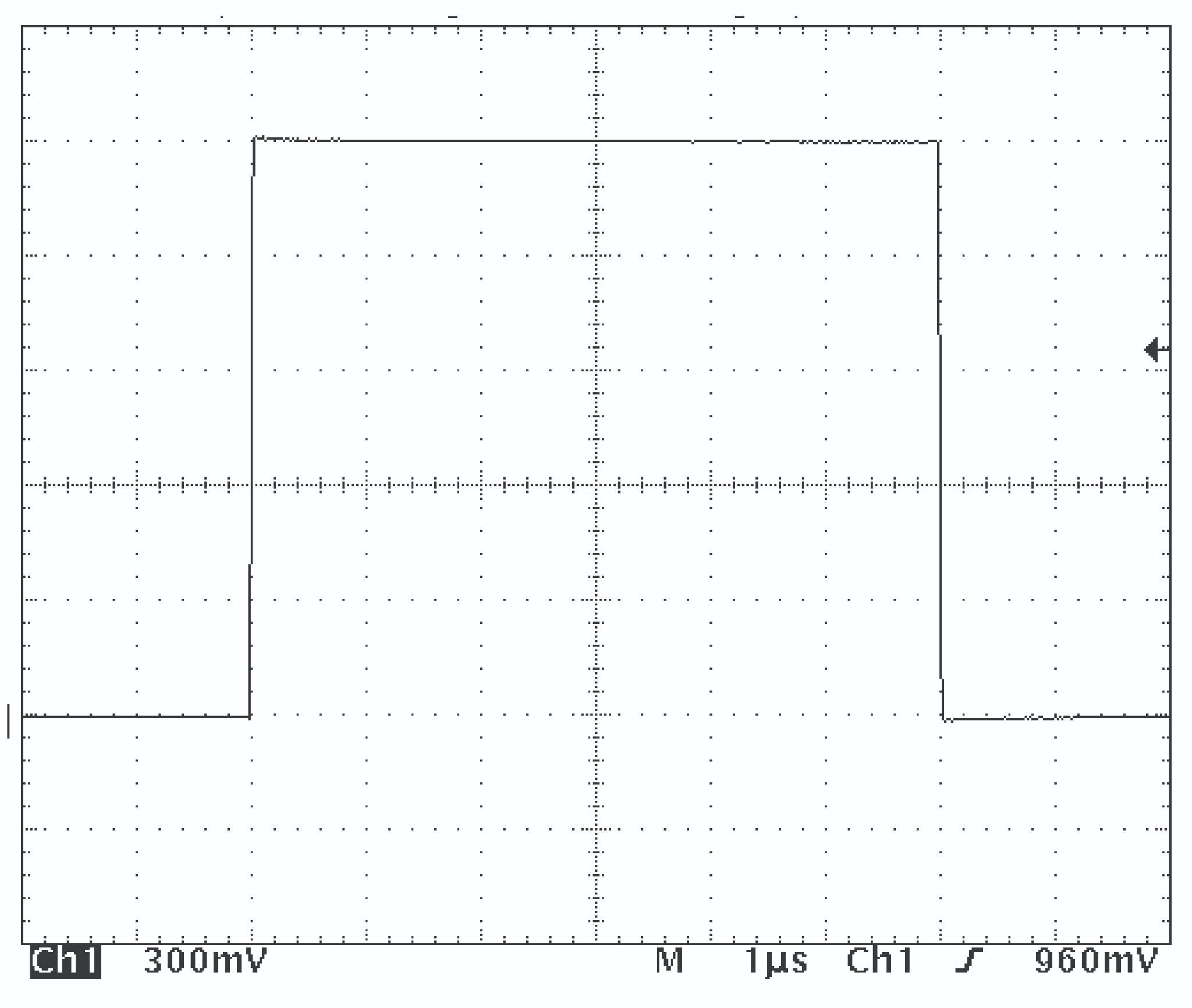
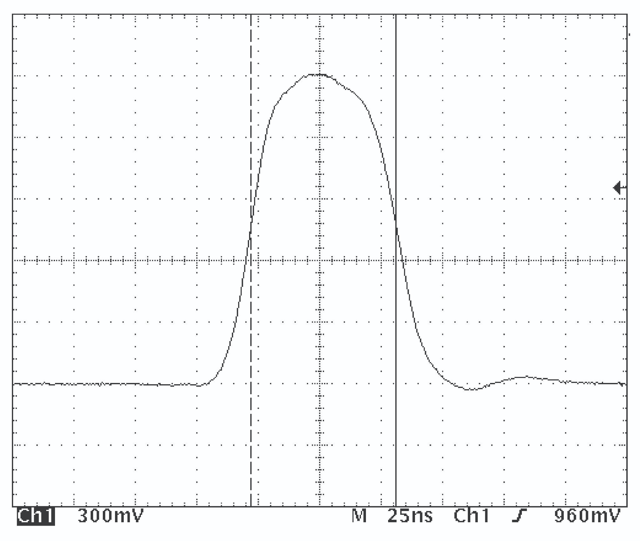
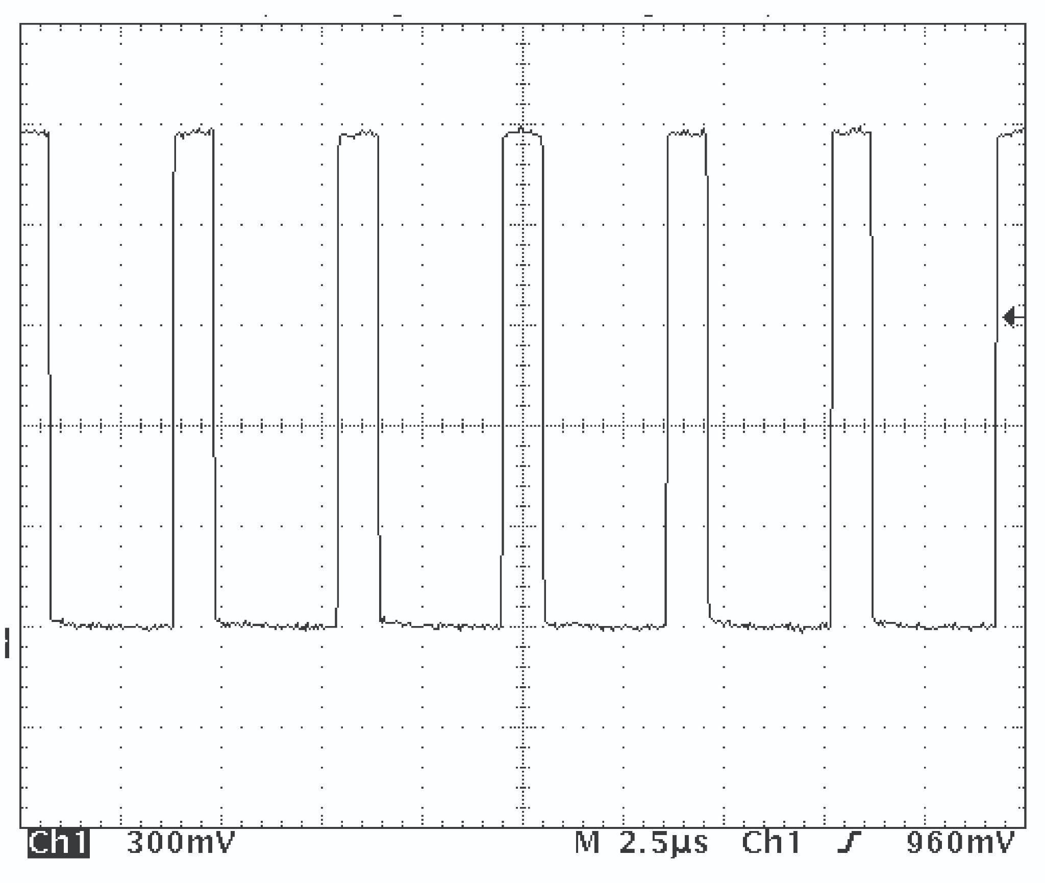
The PVX-4150 generates an output voltage pulse of 1,500 volts with rise and fall times less than 25 ns, with very flat voltage pulses to DC into a capacitive load. It can generate single-ended output pulses from ground to +1,500 V or from ground to −1,500 V, and can also generate pulses originating from a DC voltage offset from ground by using both VLow and VHigh power supply inputs. This offset can be from −1,500 V to +1,500 V, with a maximum power supply voltage differential of ≤1,500 V.
The PVX-4150 requires a TTL gate signal, a high voltage DC power supply, and optional DC offset supply inputs. The output pulse width and frequency are controlled by the gate signal. The pulse output voltage is controlled by the amplitude of the input DC power supplies.
2Operation
When the input gate is high, the VHigh supply is connected to the output. When the input gate is low, the VLow supply is connected to the output. The PVX-4150 can therefore be used to generate a negative-going pulse by logically inverting the input gate, so that the input gate is high until the unit is pulsed. When the input gate goes low, the VLow input supply is connected to the output, thereby generating a negative-going pulse.
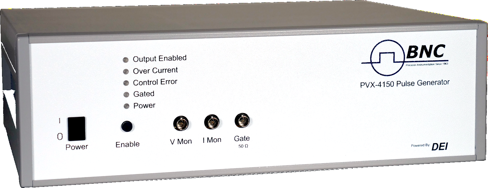
The PVX-4150 features front panel indicator LEDs to monitor the status of the pulse generator. Front panel voltage and current monitors provide a straightforward means to view the output voltage and current waveforms in real-time, eliminating the need for an external high voltage oscilloscope probe.
The pulse generator is a direct-coupled, air-cooled, solid-state half-bridge (totem pole) design, offering equally fast pulse rise and fall times, low power dissipation, and virtually no overshoot, undershoot or ringing. It has over-current detection and shut-down circuitry to protect the pulse generator from potential damage due to arcs and shorts in the load or interconnect cable. All control and protection logic circuitry, support power, energy storage, and output network are incorporated into the PVX-4150. It can be connected directly to the load, and does not require series or shunt resistors, impedance matching networks between the pulser and the load, or additional energy storage (capacitor banks). All of this is taken care of within the PVX-4150.
3Specifications
All specifications measured into a 50 pF load connected with 6 feet (~1.8 m) of RG-62 (93 Ω) coaxial cable, at 1,500 V output. The PVX-4150 can drive loads of a few picofarads to several hundred picofarads of capacitance, limited by its maximum power dissipation capability. At lower load capacitances and/or voltages less than 1,500 V, the PVX-4150 can operate at continuous pulse recurrence frequencies above 240 kHz. It can also drive resistive or inductive loads, within limitations. Contact DEI for additional information and applications assistance.
Output
| Parameter | Value |
|---|---|
| Maximum value | ±1,500 volts (VHigh − VLow) |
| Minimum value | 0 volts |
| Means of adjustment | Controlled by power supply input voltages |
| Pulse rise and fall time (10% to 90%) | <25 ns, typically <20 ns |
| Pulse width | <60 ns to DC, controlled by input gate |
| Pulse recurrence frequency (PRF) | Single shot to 240 kHz at 1,500 V continuous output, maximum limited by power dissipation (1); 5 MHz burst, controlled by input gate |
| Max. average power | 150 W (VHigh + VLow), derated at 2 W/°C over 25 °C ambient (1) |
| Max. duty cycle | Continuous |
| Droop | <1% |
| Over/undershoot | <5% |
| Throughput delay | 120 ns typical |
| Jitter | <1 ns shot-to-shot |
| Output connector and cable | SHV, with 6 feet (~1.8 m) RG-62 (93 Ω) coaxial cable |
Input DC Voltage +VIN (VHigh)
| Parameter | Value |
|---|---|
| Absolute max. value | +1,500 volts |
| Absolute min. value | −1,500 volts |
| Relative max. value | +1,500 volts over VLow voltage |
| Relative min. value | +0 V over VLow voltage |
Input DC Voltage −VIN (VLow)
| Parameter | Value |
|---|---|
| Absolute max. value | +1,500 volts |
| Absolute min. value | −1,500 volts |
| Input DC connectors | SHV, rear panel (one each for +VIN and −VIN) |
Gate
| Parameter | Value |
|---|---|
| Gate source and connector | TTL into 50 Ω, into BNC connector on the front panel |
Voltage and Current Monitors
| Parameter | Value |
|---|---|
| Voltage monitor | 1000:1 into 1 MΩ, BNC connector |
| Current monitor | 10 A/V into 50 Ω, BNC connector |
General
| Parameter | Value |
|---|---|
| Support power | 90 VAC to 240 VAC, 50/60 Hz |
| Dimensions (H × W × D, excluding connectors) | 5.2″ × 19″ × 13″ (13.2 cm × 48.25 cm × 33 cm) |
| Weight (approximate) | 18 lbs. (8.2 kilograms) |
(1) The power dissipated in the PVX-4150 when driving a capacitive load is defined by the formula CV²F (see the power budget note under Operation). This formula is not applicable when driving resistive or inductive loads.
4Front Panel & Monitoring
Front-panel indicator LEDs report the state of the pulse generator at a glance. Two monitor outputs sit on the front panel: the voltage monitor scales the output 1000:1 into 1 MΩ, and the current monitor reports 10 A per volt into 50 Ω. Together they let an engineer view the real-time output voltage and current waveforms on a standard oscilloscope, without a high voltage scope probe.
The over-current detection circuit shuts the output down on a fault from an arc or short, protecting both the pulser and the load. High voltage input and output connections are on the rear panel (SHV) to keep the operator side of the instrument at low voltage, while the TTL gate input is a front-panel BNC connector.
5Applications
- Time-of-flight mass spectrometry. Electrostatic modulation of particle beams by pulsing extraction grids and deflection plates.
- Accelerators. Modulation, deflection, and gating of charged-particle beams.
- Electro-optics. Pulsing or gating Pockels cells and Q-switches.
- Detector and tube gating. Gating microchannel plates, photomultiplier tubes, and image intensifiers; pulsing or gating power tube grids.
- Transducers. Driving acoustic transducers.
6Ordering Information
| Model | Description |
|---|---|
| PVX-4150 | ±1,500 V high voltage pulse generator; <25 ns rise/fall, <60 ns to DC pulse width, single shot to 240 kHz with 5 MHz burst, SHV output, with voltage and current monitors |
The PVX-4150 requires a user-supplied high voltage DC source and a TTL gate. A second DC supply is needed only when the output is biased away from ground. Berkeley Nucleonics can advise on supply sizing from the load capacitance, pulse voltage, and repetition rate.